Design of humanoid artificial hand control system combining FPGA and DSP
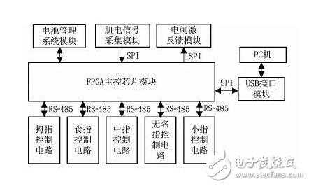
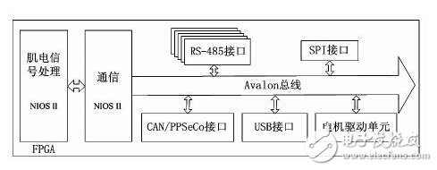
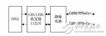
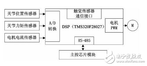
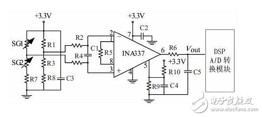
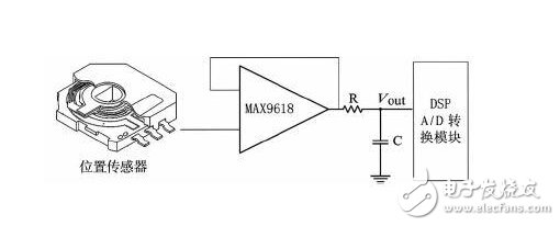
The humanoid artificial hand has the major social needs as the main target of rehabilitating the human hand function as a disabled patient. The ideal artificial hand should have the bionic characteristics of the human hand, mainly reflected in the three aspects of artificial hand construction, control mode and environmental perception. However, due to its limited volume and complex sensor system, the control system is put forward higher requirements. The existing control systems are available in both external and built-in versions. External control systems are mostly used for research-type artificial hands, such as Cyber ​​Hand, Tokyo Hand, Vanderbilt Hand, etc. This control system is mainly used for the verification of algorithms and solutions, and it is less popular in the application of disabled people. The built-in control system is used in both research-type fake hands and commercial fake hands. The research-type artificial hand control system invests heavily in environmental perception and two-way information interaction, such as Smart Hand, DARPA hand; while commercial fake hand control system There are also some integrated external sensors, but the sensor system is simple, and there is a big gap in two-way information interaction, such as i-Limb, BeBionic Hand. The HIT IV generation of false hand control system uses DSP as the main control chip, integrated with position sensor and torque sensor to sample the EMG signal. However, the control system is a whole and large, and it is only suitable for HIT IV generation fake hands. The DSP chip is weaker than the FPGA in function expansion, which is not conducive to secondary development. In this paper, the modular design scheme is adopted, and FPGA is used as the core chip. The modules of motion control, EMG signal acquisition and electrical stimulation are independently designed and connected through a common interface. On this basis, multi-modal multi-finger capture experiments were conducted. 1 imitation artificial hand system introduction The control system designed in this paper is controlled by HIT V. The hand is slightly smaller than the adult hand, with 5 fingers, 2 knuckles for each finger, and an internal rotation/abduction joint for the thumb. There are 11 active joints, and the whole hand is driven by 6 DC motors. Each finger is equipped with a torque sensor, a position sensor, and a fingertip six-dimensional force sensor. The control system adopts the modular design idea, divides the whole system into several modules, establishes interconnection with each other through the common interface, so that the whole control system can be placed inside the humanoid artificial hand to realize mechatronics. 2 FPGA-based control system design The humanoid artificial hand control system is used to realize the driving control of each finger of the artificial hand, the collection of various sensor information, and the communication with the upper computer (PC or PCI control card). The control system is composed of 10 modules, which are: a main control chip module composed of an FPGA, a USB interface module, a thumb control circuit module, an index finger control circuit module, a middle finger control circuit module, a ring finger control circuit module, a little finger control circuit module, EMG signal acquisition module, battery management system module, electrical stimulation feedback module. The modular design approach increases the flexibility and independence of the control system, making it easy to debug and modify the module separately. The overall functional block diagram of the electrical system is shown in Figure 1. Figure 1 Functional block diagram of the electrical system 2.1 FPGA main control chip module design The FPGA main control chip module uses Altera Cyclone III series FPGA chip EP3C25F25617 as the control core, responsible for the processing of EMG signals and various sensor signals, communication with finger circuits, USB communication, CAN communication interface and other functions. At the same time, the main control chip module is also responsible for the control of the thumb internal rotation/abduction degree of freedom driving motor. Each function is written in VHDL language. The dual NIOS core embedded in the FPGA constitutes a dual-core processor. One NIOS core is used for EMG signal processing, and the other NIOS core is used for communication. The dual core communicates through 2M EEPROM. FPGA functional block diagram is shown in Figure 2. Figure 2 FPGA functional block diagram RS-485 communication is realized by controlling the RS-485 transceiver interface chip MAX3362 in the NIOS core with the custom component AutoSCI. The MAX3362 transceiver chip enables high-speed data transfer with a 3.3 V low voltage. CAN and LVDS communication adopts the multiplexing circuit design (Fig. 3), and the function conversion is completed by replacing the receiving and transmitting interface chip. CAN communication uses TI's CAN transceiver SN65HVD230QD as an interface chip. LVDS communication uses TI's half-duplex LVDS transceiver interface chip SN65LVDM176 to form a PPSeCo high-speed serial communication system to communicate with the PCI control card. The communication rate can reach 25 Mbps, ensuring the timeliness of control information and sensor information transmission. Figure 3 CAN communication / LVDS communication multiplexing circuit The thumb internal rotation/abduction degree of freedom drive motor is controlled by the custom component PWM in the NIOS core. The component function is written in VHDL language, and the PWM wave period and duty cycle are adjustable. The motor drive chip uses the MPC17531A, which integrates a double H-bridge to directly control the DC brush motor. 2.2 finger motion control module design The five-finger motion control module uses the same design to enhance system interchangeability and versatility. The module is controlled by DSP as the control core. The DC brushed motor drive chip MPC17531A is used as the motor drive chip. It is responsible for the driving of the finger motor, the acquisition and processing of the torque sensor, position sensor and motor current sensor signal, and the communication with the tactile sensor system. Finally, Each data communicates with the main control chip module through the RS-485 communication interface. The control module is shown in Figure 4. Figure 4 Functional block diagram of the finger motion control module The DSP TMS320F28027 used in this module has a high running speed and a small package. The internal integrated 16-channel 12-bit A/D converter enables sampling of torque, position, and motor current signals. The serial asynchronous communication interface communicates with the main control chip module through the RS-485 transceiver interface chip. EPWM module can directly control DC brush motor drive chip MPC17531A. As shown in FIG. 5, the joint torque sensor signal acquisition system includes a torque sensor, a processing amplifier circuit, a filter circuit, and an A/D conversion circuit. The torque sensor is based on the strain principle. The instrumentation amplifier INA337 is used to form a half-bridge circuit to amplify the torque signal and then enter the A/D conversion chip through the RC filter circuit. Figure 5 torque sensor signal acquisition system As shown in FIG. 6, the joint position sensor signal acquisition system includes a position sensor, a processing amplifier circuit, a filter circuit, and an A/D conversion circuit. Based on the principle of rotary potentiometer, the position sensor uses the integrated operational amplifier MAX9618 to amplify the potentiometer signal and then enter the A/D conversion chip through the RC filter circuit. Figure 6 position sensor signal acquisition system 2.3 EMG signal acquisition module design The EMG signal acquisition module is used to collect the signal of the EMG electrode and the signal filtering and D/A conversion and store it in the CPU, including the filter circuit composed of the RC circuit, the D/A conversion circuit and the voltage conversion circuit. The digital signal is converted to 3.3 V by a voltage conversion chip and input to the CPU central processor via the SPI interface. 2.4 battery management system module design The battery management module includes a battery, a current sensor, a buzzer circuit, and an LED display circuit. The current sensor monitors the battery output current in real time, and displays the charging status and low battery alarm through the LED display circuit and the buzzer circuit.
The solar power supply system USES photovoltaic cells to convert solar energy into electricity, which is used to power electrical appliances and batteries by stabilizing the system. The voltage of the photocell output is too large for light, so it must be stabilized before it can be used. Cell phone battery storage is ok, but consider the voltage and capacity of the battery.Anti-reflective Coated glass along with UV-T UV-C encapsulant ensure higher transmission efficiency. •Higher efficiency cells (+18%) for more power output •Positive power output tolerance (+5%) •PID resistant Cells encapsulants yield efficient performance under hot humid weather. •Resistant to salt mist corrosion. •IP65 / IP67 rated junction box with 3, 25 A diodes, giving 15A box rating. •Certified for 1500 V system voltage .
Poly 150W Solar Panel,150W Solar Panel,150 Watt Solar Panel Yangzhou Bright Solar Solutions Co., Ltd. , https://www.solarlights.pl