Design of Flight Control System for UAV Based on DSP
With the development of science and technology and the transformation of military strategy, unmanned aerial vehicles have a wide range of application prospects and extremely important practical significance in the military and civilian fields. Countries are developing and developing various unmanned aerial vehicles with unique capabilities. The core of the transformation is the flight control system. With its rich instruction system, high-speed and high-precision computing capabilities, and rich on-chip peripheral resources, DSP provides a good platform for the development of flight control systems. TMS320F2812 (hereinafter referred to as F2812) selected by this system is a 32-bit DSP chip developed by TI. It adopts high-performance static CMOS technology and can work up to 150M ips. On-chip integrated 128K word FLASH memory for easy software upgrade; also integrates rich peripheral devices such as: 12-bit 16-channel A/D converter with sampling frequency up to 12. 5M IPS, two motor-oriented events Manager and a variety of standard serial communication peripherals. Based on this, a new type of flight control system with high precision, scalability, miniaturization, and low cost is designed. 2 Hardware System Requirements and Design The key to the hardware design of the flight control system based on DSP lies in the overall design of the system. Interface design is an important link that will directly affect the performance of the system. In order to reduce the burden on the system, the external input signal is read in an interrupt mode, and the signal input and output must be considered for noise immunity. Taking full account of the on-chip resources of the TMS320F2812 and the interface requirements of the system, only a small number of external interface extensions to the DSP chip are required to satisfy all the functions and future expansion requirements of the flight control system. At the same time, due to the system's large amount of input logic, A ltera CPLD chip EPM7128 is used to complete the data processing and logic operation functions to reduce the volume of the control circuit, increase the reliability of the system, and realize the monitoring and control of the status of each unit of the control system. . The overall system design is shown in Figure 1. The following will explain the implementation of each module of the system. Figure 1 overall system hardware design 3 hardware implementation 3. 1 analog signal reception The analog signal is input through the signal conditioning module. The A/D converter selects the 12-bit successive approximation of the A/D converter AD1*. The on-chip 3-bit output buffer circuit and the high-precision reference voltage source and clock circuit have their own sample-and-hold. The design of the connection used in this design is shown in Figure 2, which allows AD I* to operate in full control mode. In the use of AD1*, program start, marker query, start signal and conversion end signal are used in conjunction to make AD I* in the data output state once the conversion is completed. At the same time, the AD end flag is generated to increase the pass rate when multi-channel is used. Figure 2 A / D expansion circuit block diagram. 3. 2 serial port communication The F2812 processor provides two serial communication interfaces (SC I) that support 16 receive and transmit FIFOs. However, it still cannot meet the communication requirements of the flight control system and multiple peripherals. Therefore, the system selects the asynchronous serial interface extension chip SP2338 to easily expand the SC I1 of the DSP into three full-duplex, asynchronous serial communication interfaces with baud rates up to 9600 b/s, serving as the main controller and dedicated. Communication equipment data transmission channel, control system and ground communication transmission, SC I2 as GPS and CPU communication channel. The SP2338 is simple to use, does not require the support of the underlying software, and can work on power-up. The expansion of the serial port is shown in Fig. 3. ADR I0 and ADR I1 are downlink address lines, ADR I0, ADR I1= 00, 01 and 10 are respectively corresponding to the sub-serial 0, and l 2; ADRO0 and ADRO1 are uplink address lines, ADRO0 and ADRO1. - 00, 01, 10 correspond to sub-serial 0, 1, 2 respectively. The F2812's I/O port is directly connected to the SP2338's address line. When sending data, the DSP changes the downstream address by changing the state of the I/O port, and selects a specific sub-serial port. When receiving data, the DSP determines the specific serial port of the data by reading the status of the I/O port. Read the data to make corresponding treatment. Therefore, system efficiency can be improved and software consumption can be reduced. The RS232, RS422, and RS485 communications can be achieved by applying a level-shifting chip. 3. 3 Memory Expansion The F2812 contains 128K16-bit FLASH memory. Considering capacity and speed, the system must be expanded with memory. A 64K word IS61LV6416 memory chip manufactured by ISSI was used as program expansion memory. + 3. 3V power supply, maximum access time is less than 12ns. No additional delay circuit is required, and the data and address lines are directly connected to the data lines and address lines of the DSP. The 51 pin R/W of DSP is connected with the chip select signal CE pin of 61LV6416, and the read and write strobe signals of DSP are respectively connected with the read and write strobe signals of 61LV 6416. 3. 4 PWM wave output The servo of the UAV servo is controlled by the PWM (Pulse Width Modulation) signal. Using the change of the duty cycle, multiple parallel PWM signals generated by the DSP are added to the servo control circuit of the signal isolation drive, by changing the servo's Location for control purposes. The TMS320F2812 integrates a PWM control signal generator and each event manager can generate eight PWM outputs. Since the PWM output of the TMS320F2812 chip is +3.3V, and the high level of the servo control signal input PWM pulse width modulation signal needs +5V, the high level of the pulse width modulation signal output from the DSP needs to pass the level. Only after the conversion can the steering gear work. In order to avoid the interference of the motor drive board to the main control board, the high-speed opto-isolated device 74LS245 is used to isolate the PWM signal and block the conduction interference of the motor drive board to the main control board. 3. 5 reset, power circuit In the entire hardware design, the main DC power supplies used are +1.8V, +3.3V, +5V, and +12V. The on-board power supply adopts TI's TPS767D318, through 5V regulated power supply, provides the required voltage of DSP of 1. 8V and 3. 3V voltage required for DSP and peripheral circuit. When all the signals are connected to the F2812, the level matching problem must be considered and the buck chip must be used to solve the problem. The +12V DC power supply is provided by the battery. Other DC voltages can be obtained through the DC/DC converter module. The +5V voltage is obtained with the integrated voltage regulator module LM7805. Taking into account the need to 1. 8V and 3. 3V two voltages in this system, so select the IDT company's LM1117 chip to 5V voltage input to the DSP level conversion, can make 5V input voltage is reduced to 1. 8V and 3 . 3V. The LM1117 provides current limit and thermal protection. All power supplies on the target board can be supplied with a 5V regulator module. In addition, the system is provided by TI's TPS3307 for manual reset for ease of debugging. After the reset signal is decoded by the CPLD, it outputs two levels, high and low, and resets the components that require different reset levels. All reset sources of the manual button and the AT bus are introduced into the CPLD, driven by the built-in R eset Log ic of the CPLD, and output to the reset destination. 4. System software design The software system adopts the embedded real-time operating system DSP / B IOS integrated in CCS of TI's DSP integrated development tool and adopts mixed programming of C language and assembly language. The system initialization module sets the operating mode of SJA1000, and its initialization can only be performed in reset mode. The initialization flow chart is shown in Figure 4. Figure 4 Initialization process block diagram. System control flow chart shown in Figure 5. The data storage is placed in the task thread, and the process is to store the flight data analysis results in F lash . The detection task thread can be completed by the periodic function PRD. The PRD can determine when the function is running based on the real-time clock. Here, the test task 100m s is set to run once. Figure 5 System Control Flowchart. The starting of all tasks is closely related to the small cycle count on the flight control system bus. The tasks related to receiving the bus data are initiated by the message distribution thread. When the received message is the synchronous data code sent by the PSP, the terminal object synchronizes itself. The small cycle counts, and start the corresponding task according to the current small cycle. All the tasks are contained in the message processing thread. Each terminal has one such thread. Each thread works independently and makes each terminal work in parallel. All the logic control functions of the system adopt the cycle operation mode and wake up by the timer interrupt program every 10ms. CPLD is used for logic operation and data processing, and the analog input signal is detected to determine the working status of each monitoring object and the output quantity is determined according to the system control logic. It informs the DSP when its status changes, assisting the DSP in completing the system's self-detection function. In the condition monitoring, the current detected state quantity is compared with the stored previous state quantity. If the two states are the same, no operation is performed; if there is a change, an interrupt signal INT is sent to the DSP to notify the DSP to read. data. When receiving the control instruction sent by the DSP, the instruction is compared with the current state, and if it is in compliance, the control instruction is no longer sent, thus preventing malfunction caused by multiple times of sending the control instruction. During the flight process, the tasks of the control system mainly include collecting the attitude data of the drone, calculating the control quantity and outputting it to an actuator such as a steering gear, receiving the instruction of the ground station and transmitting the position of the unmanned aerial vehicle. Using the designed control board to implement the servo control algorithm and complete the control of the actuator steering gear. Figure 6 shows the PWM control signal waveform of one of the servos output by the control system. 5 Concluding remarks Using multi-peripheral high-performance DSP chip TMS320F2812 combined with CPLD, and using DSP / B IOS as real-time operating system for real-time multi-tasking design, effectively improving the reliability and real-time performance of the system. After debugging, the system has stable performance in actual operation and meets the design requirements. The system is small in size, light in weight and low in cost. It has a certain degree of expansibility and is suitable for constructing small unmanned aerial vehicles with strong real-time performance, miniaturization, and low cost. 51V Battery Pack,Portable Battery Box,Portable Battery Bank,Ac Battery Pack Zhejiang Casnovo Materials Co., Ltd. , https://www.casnovonewenergy.com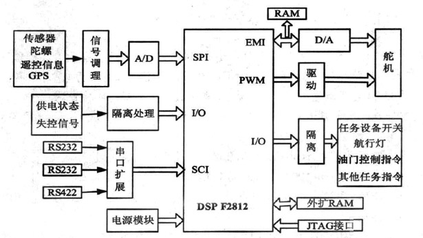

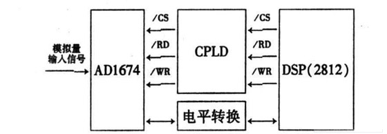
Figure 3 Serial port expansion block diagram. 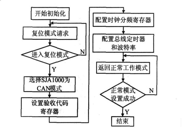
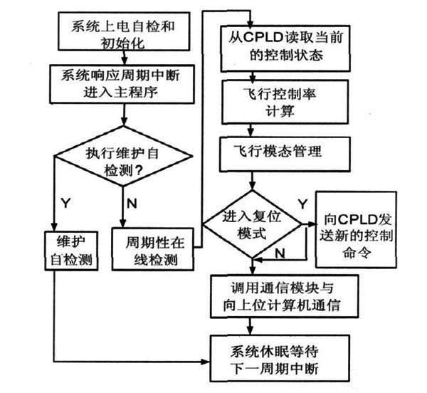

Figure 6 Servo control signal.