Xilinx Programmable Logic Device Design and Development (Basic) Serial 8: Spartan
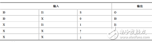
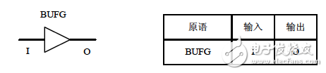
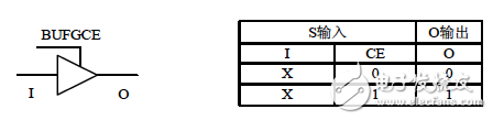
The Spartan-6's clock buffer/multiplexer (BUFG or BUFPLL) can directly drive the clock input signal to the clock line or switch between two uncorrelated signals or even asynchronous clock signals through a multiplexer. The primitives of the global clock buffer are shown in Table 2-7. Table 2-7 Primitives for Global Clock Buffer/Multiplexer The BUFGMUX can be switched between two clock sources as a BUFG or as a multiplexer for two global clock sources. BUFGMUX only drives global clock routing resources. General-purpose routing resources can also drive clock inputs on FPGA logic flip-flops, but are generally not recommended because of the high SKEW of general-purpose routing resources. As shown in Figure 2-6, BUFGMUX is a clock buffer with two clock inputs I1 and I0, a clock output O, and a select line S. This eliminates the glitch generated when switching between two clock sources. The selection line S must meet the settling time requirement, and violation of this settling time may result in a glitch signal. When select line S flips to select another clock source output, the output remains in an inactive state until the next valid clock edge comes. When two clocks are switched, the output level can be high or low, and the default is low. The cross decoupling registers ensure that the BUFGMUX output does not generate a clock edge. The S input is low, the clock input I0 is selected; the S input is high, and the clock input I1 is selected. BUFGMUX also has built-in programmable polarity, equivalent to switching I0 and I1. Each flip-flop can set the polarity of the clock signal to determine the rising or falling edge trigger to avoid generating two different clock signals. Table 2-8 BUFGMUX function table BUFGMUX_1 and BUFGMUX have the same function, except that BUFGMUX_1 is sensitive to rising edges and remains High until the input is switched. As shown in Figure 2-7, BUFG is actually a clock buffer with a clock input and a clock output. It is also a common primitive for clock buffers in Virtex and Spartan devices. Figure 2-7 Primitives of BUFG BUFGCE is a clock buffer with one clock input, one clock output, and one clock enable line. When the clock enable CE is high, the input I is buffered; when CE is low (inactive), the output O is low. Its primitive is shown in Figure 2-8. Figure 2-8 Primitives of BUFGCE BUFGCE_1 has the same function as BUFGCE, except that when the clock enable CE is low, the input I is buffered; when CE is high (inactive), the output O is high. Usb Megaphone,Megaphone With Usb,Megaphone With Bluetooth,Megaphone With Usb Port Shangqiu Huayitong electronic technology co., Ltd. , https://www.huayitongmegaphones.com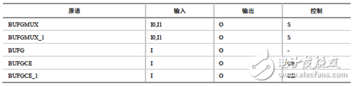
When the S input changes, the output remains Low until another (to be selected) clock changes from High to Low. Then, the new clock starts to drive the output. As shown in Table 2-8, since the first low-to-high transition output of the input does not flip, the output will not be shorter than the shortest input clock pulse.