Learn more about the principle of crystalline silicon cell power generation
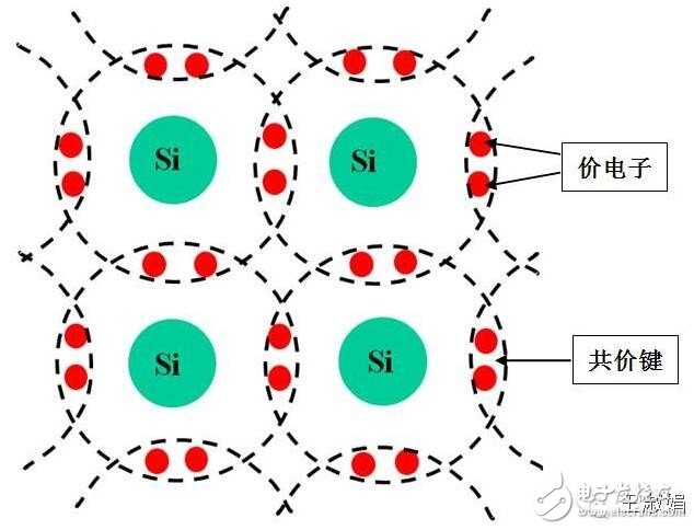
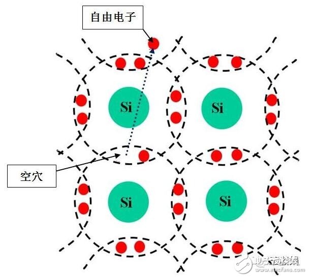
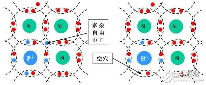
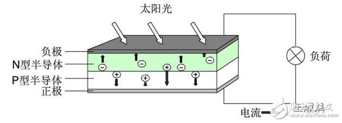
Discussing photovoltaic power generation every day, do you know the principle of solar cell power generation? This paper introduces the power generation principle of crystalline silicon solar cells in text form. It belongs to the popular science level and is very easy to understand. Solar cell power generation principle 1. N-type semiconductor and P-type semiconductor A completely pure semiconductor with a crystal structure, called an intrinsic semiconductor, forms a covalent bond between atoms, and its structure is shown in Figure 1-3. The two electrons in the covalent bond are called valence electrons. Figure 1: Intrinsic semiconductor structure After obtaining a certain amount of energy (increased temperature or exposure to light), the valence electrons can break away from the bond of the nucleus and become free electrons (negatively charged), leaving a vacancy in the covalent bond, called a hole (positively charged). , as shown in Figure 1-4. Both free electrons and holes are called carriers, and the number of carriers in the intrinsic semiconductor is extremely small, and the conductivity is poor. Figure 2: Formation of free electrons and holes after valence electrons are excited The intrinsic semiconductor is doped with a small amount of impurities (some elements) to form an impurity semiconductor, which can greatly enhance its conductivity. Incorporating a pentavalent phosphorus element to replace a silicon atom, four of the five outer electrons of the outer layer of the phosphorus atom form a covalent bond with the surrounding semiconductor atoms, and an extra electron is almost unbound, making it easier to become a free electron. . Therefore, the number of free electrons after doping is greatly increased, and free electron conduction becomes the main conductive mode of such a semiconductor, which is called an N-type semiconductor. When a trivalent boron element is substituted for a silicon atom, and the three outer electrons of the outer layer of the boron atom form a covalent bond with the surrounding semiconductor atoms, a "hole" is generated. Therefore, the number of holes after doping is greatly increased, and hole conduction becomes the main conduction mode of such a semiconductor, and is called a P-type semiconductor. N-type or P-type semiconductors are neutral and have no external electrical properties. Figure 3-1a: N-type semiconductor Figure 3-2b: P-type semiconductor The electrons of the N-type semiconductor are many, and the holes are few; The holes of the P-type semiconductor are many, and the electrons are few. Second, "PN knot" and "photovoltaic volt effect" The PN junction is composed of an N-doped region and a P-doped region in close contact. On a complete silicon wafer, a different doping process is used to form an N-type semiconductor on one side and a P-type semiconductor on the other side, and a region near the interface between the two semiconductors is a PN junction. The basic structure of a solar cell is a large-area planar PN junction. When sunlight hits the PN junction, the PN junction absorbs light to excite electrons and holes, and generates a voltage in the PN junction, called the "photovoltaic effect" or simply "photovoltaic effect." Figure 4: Principles of photovoltaic power generation
Film capacitors are electrical capacitors with an insulating plastic film as
the dielectric, sometimes combined with paper as carrier of the electrodes.
These plastic films are sometimes metalized and are available in the market
under the name metalized Film Capacitor,these capacitors are sometimes also
called plastic capacitors.
Film Capacitor,X-Ray equipment Capacitor,Axial Polyester Capacitor,Polypropylene High Voltage Capacitor XIAN STATE IMPORT & EXPORT CORP. , https://www.capacitorhv.com