THS4271 Integrated Test Circuit Characteristics and Applications
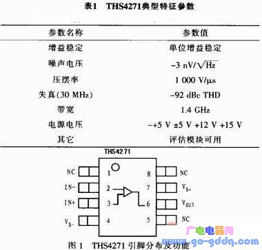
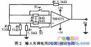
Based on the integrated operational op amp THS4271 produced by TI, the experimental test circuit is built. Under the defined conditions, the input offset voltage UIO of the op amp, input offset current IIO, common mode rejection ratio CMRR, open-loop differential mode are measured. Magnification AUd and other main parameters. At the same time, the corresponding parameters corresponding to the measured data are simply analyzed. Based on the THS4271 unit gain stability, low distortion, high-pressure slew rate and other characteristics, several application examples are given to illustrate its application value in some engineering fields for future users. Although after years of development, integrated circuit op amps are still widely used in modern integrated circuits and system-on-chips (SoCs), and often require severe demands on their performance. So research around high-performance integrated circuit operational amplifiers has been enduring. In this paper, the main parameters of the THS4271 integrated operational amplifier are tested in combination with the actual project requirements. The results and their applications are discussed, which is beneficial to the future development of the experiment and provides reference for the users of the device. 1 chip introduction The THS4271 is a low noise, high slew rate, unity-gain stable voltage feedback amplifier manufactured by TI. Its normal operating voltage range is 5 to 15 V. Combining low noise, high slew rate, wide bandwidth, low distortion and unity gain stability, the THS4271 delivers high performance. The user of this amplifier can achieve the higher dynamic range required for the experiment over a wider frequency band without having to worry about the stability of the amplifier during the loss period. The amplifiers in this family are available in SOIC, MSOP with PowerPAD, and MSOP with PowerPAD leadless. Typical characteristic parameters of THS4271 are shown in Table 1. The original shape, pin distribution and function of each pin of THS4271 are shown in Figure 1. (where NC stands for hanging) 2 Experimental principle 2.1 Input offset voltage When the input signal of an ideal operational amplifier (referred to as an op amp) is zero, its output DC signal should also be zero. However, in fact, if there is no external zeroing measure, the output voltage is often not zero because the internal parameters of the op amp are not completely symmetrical. The phenomenon that the output is not zero when the input is zero is called the offset of the integrated op amp. At room temperature and standard supply voltage, in order to make the DC voltage at the output terminal zero, a DC voltage must be added to the input terminal as the compensation voltage to offset the output voltage from the zero point. This voltage applied to the input terminal is called input. Offset voltage UIO. Obviously, the smaller the UIO value, the better the symmetry of the parameters of the op amp. 2.2 Input offset current The bias current of the op amp refers to the base currents IB1 and IB2 of the differential pair of the op amp input stage. Due to the dispersion of the transistor parameters, IB1 ≠IB2. When the input signal is zero, the difference between the base bias currents of the two inputs of the op amp is called the input offset current, IIO, ie IIO=|IB1-IB2|. Obviously, the presence of IIO will shift the output zero point. The higher the signal source impedance, the more serious the offset current is. 2.3 Common mode rejection ratio The common mode rejection ratio is a parameter used to characterize the magnitude of the op amp's ability to reject common mode signals. Defined as the ratio of the differential mode voltage amplification factor Ad of the op amp to the common mode voltage amplification factor Ac: CMRR = Ad / Ac; expressed in decibels: CMRR = 20 lg (Ad / Ac) dB. The common mode rejection ratio is an important parameter in the application. The output of the common mode output of the ideal op amp is zero, but in the actual integrated op amp, the output is unlikely to have no common mode signal component. The smaller the mode signal, the better the circuit symmetry, and the stronger the immunity of the op amp to the common mode interference signal, that is, the larger the CMRR. 2.4 Open-loop differential mode amplification The DC differential mode amplification factor of the integrated operation without external feedback is called the open-loop differential mode voltage amplification factor, which is represented by Aud. Defined as the ratio of the open-loop output voltage amplitude UO to the applied signal voltage amplitude Uid between the two differential inputs: AUd=UO/Uid. 3 test circuit, data and analysis 3.1 Input offset voltage measurement The schematic diagram of the offset voltage test circuit is shown in Figure 2. Close the switches S1 and S2 (use the wire instead of the experiment), make the resistance Ra short, measure the output voltage UO at this time is the output offset voltage, convert to the input, you can get the input offset voltage UIO=R1·UO/(R1 +Rf), measured by UO=385 mV, and brought into the above formula to obtain UIO=3.85mV. Tn Panel,Tn Lcd Display Module,Tn Positive Lcd Display Module,Tn Lcd Display Module Connector Huangshan Kaichi Technology Co.,Ltd , https://www.kaichitech.com