Analysis of sandwich resistance structure and principle characteristics
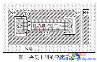
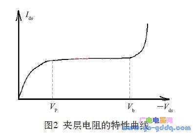
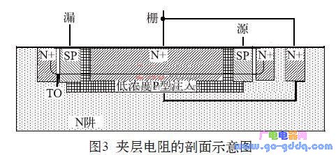
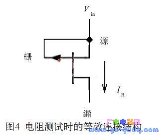
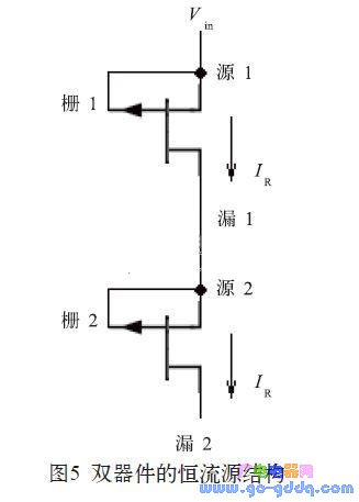
1 Introduction In the circuit design of an integrated circuit, especially in the design of an analog circuit, it is inevitable that a resistor is required. For low-resistance applications, aluminum wire resistors, polycrystalline resistors, N+ resistors, or P+ resistors can be used. For a larger resistance, it can be realized by an N-well resistor, a P-well resistor, or a high-resistance polycrystal. For higher resistance requirements, or high resistance requirements but small footprint and low precision requirements, this can be achieved with an inverted MOS tube or sandwich resistor. As the name implies, the interlayer resistance is the resistance sandwiched by other layers. The resistance of the interlayer resistor is generally 5~50 kΩ. With the increase of voltage, it can reach 100 kΩ or higher. 2 sandwich resistance structure and principle characteristics analysis 2.1 Structure of the sandwich resistor There are many ways to achieve sandwich resistance in an integrated circuit process. The sandwich resistance studied in this paper is one of them, and it does not need to be added by additionally adding a lithographic MASK layer. Figure 1 is a schematic plan view of the interlayer resistance. In Figure 1, the interlayer resistance region is a low concentration P-type implant region, which is mainly implemented using existing layers in the process, such as the Pbase layer or the Pbody layer. The P-type interlayer resistance region is completely surrounded by N+ and N-wells, so the structure is a P-type sandwich resistor sandwiched between two layers of N+ and N-well. 2.2 Characteristics of the sandwich resistor The advantage of the sandwich resistor is that the resistance is high, and the disadvantage is that it is sensitive to voltage. The sandwich resistance was subjected to IV scanning with a starting voltage of 0 V and a step of 0.5 V. The result was found as follows: When the voltage across the resistor increases from 0, the resistance of the interlayer resistor rises rapidly, but the voltage exceeds 4 After V, the resistance value continues to increase, but at this time it exhibits a linear rise characteristic, that is, the resistance follows the voltage proportionally. When the voltage reaches about 14~15 V, the resistance begins to decrease sharply, showing a blow. Wear effect. Curve the IV value of the above resistance test to obtain the graph 2. In Figure 2, the inflection point Vp is about 4 V, and the inflection point Vb is about 14 to 15 V. 2.3 Principle analysis of sandwich resistance Observe the curve and find that it is very similar to the output characteristic curve of the MOS tube. Further analysis of its longitudinal structure found that the interlayer resistance can be understood as a P-channel JFET tube (junction field effect tube), and its longitudinal section is shown in Figure 3. In Figure 3, the channel region of the JFET tube is a low-concentration P-type implant region, and the P-type channel is sandwiched by the N+ and N-wells. Therefore, the N+ and N-well can be regarded as the gate of the JFET tube. Think of one of the two SP injection areas as the source of the JFET tube and the other as the drain of the JFET tube. Therefore, in FIG. 2, the inflection point Vp is the pinch-off voltage of the P-channel JFET tube. When the -Vds voltage exceeds Vp, the JFET tube is pinched off, and the source-drain current begins to stabilize. The inflection point Vb is the breakdown voltage of the P-channel JFET tube. When the -Vds voltage is greater than Vb, the JFET tube generates a breakdown and the Ids increases. In the previous sandwich resistance test, the gate and gate of the PJFET tube were actually shorted to form the connection structure shown in FIG. As can be seen from FIG. 4, as long as the gate source of the JFET tube is shorted and connected to the input operating voltage Vin, when the voltage changes between Vp and Vb (ie, Vp) In general, Vp is around 3~4 V, and Vb can be around 10~15 V or even higher. Of course, the size of Vp and Vb will be different due to the difference between different processes. The single device current source can output a constant current when the input voltage varies between 4 and 15 V. In order to obtain a wider voltage range, the above circuit needs to be improved, as shown in Figure 5. Shaded Pole Motor,Capacitor Motor Yc Series,Capacitor Motor Tl61,Shaded Pole Ac Motor Wentelon Micro-Motor Co.,Ltd. , https://www.wentelon.com