Video Cache Design Based on MIMO Technology
Abstract: Based on Xilinx DDR IP, MIMO technology is used to design a multi-input and multi-output buffer for controlling DDR SDRAM in EQAM modulator. A network model is given to improve resource consumption, and actual tests show that the expected design requirements are met. This article refers to the address: http:// Glass Aquariums,Aquarium Fish Tank,Glass Turtle Tank,Glass Fish Tank Sensen Group Co., Ltd.  , https://www.sunsunglobal.com
Keywords: DDR; MIMO; EQAM buffer
With the continuous development of high-speed processors, the field of embedded system applications is more and more extensive. High-speed large-capacity buffers are widely used in audio and video systems. However, dedicated high-speed large-capacity cache chips are too expensive, and traditional SDRAMs are used in bandwidth. It has gradually failed to meet the application requirements, especially when multiple data is multi-input and multi-out, neither of them can meet the requirements well. Here, a design using double-edge random dynamic memory (DDR SDRAM) combined with dedicated dedicated circuit is proposed. Program.
Designed for use in DVB-C-based EOAM modulator systems, the basic requirements of the system are to buffer Gigabit IP data from multiple video streams and to multi-channel high-speed IP data. The input is 2 Gigabit networks. Port, output to hundreds of data distribution channels of the RF interface.
In the past system design, it was proposed to use a common SDRAM chip as a physical buffer unit, but due to the limitation of the working speed of such a chip, under the condition of basic bit width, the high bandwidth requirement of the above system is not achieved. If the chip speed is not increased, the bit width is simply increased. Because the delay of each data is different, and the transition of the 3.3 V voltage rising and falling edge of the SDRAM is wide, the stable time window of the chip data sampling is narrowed, and the data transmission is performed. The reliability is degraded; at the same time, as the bit width increases, the number of pins increases, causing a linear rise in design complexity. In this paper, DDR SDRAM is used as the storage unit. By using the clock double edge transmission data without changing the system clock, the transmission bandwidth of the same frequency chip is doubled on the basis of SDRAM, which satisfies the needs of high bandwidth buffer. .
1 DDR Memory Introduction DDR memory is a dual data rate synchronous dynamic random access memory. Like the early single data rate synchronous dynamic random access memory, the internal memory unit uses capacitor charging to store data. Therefore, the capacitor must be constantly charged to maintain data. This is called "refresh". The SDRAM data bus accesses data on the rising edge of each clock, while the DDR SDRAM accesses data on both the rising and falling edges of each clock, so that the data bus bandwidth is constant with the same data bus width and clock frequency. Doubled the gain.
2 system design The design uses Xilinx's Sptan3a-dsp 1800a as the main controller, using Micron's MT64V32X16 chip as the storage medium, the maximum storage capacity is 512M. The logic part of the system consists of arbitration module, input buffer module, scheduling decision module, address conversion module and DDR interface control module. The block diagram is shown in Figure 1. 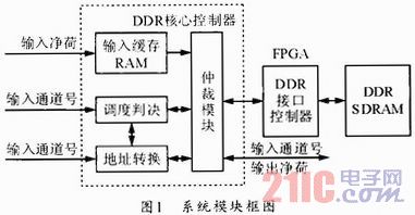
The arbitration module in the core controller generates the corresponding control commands. After the power-on initialization reset, and during the system running, the refresh command, the write operation command and the read operation command are issued for the work priority; the DDR interface control module implements the core controller command according to the basic timing of the DDR chip operation. For the information transmission of the physical chip; the south DDR chip has non-real-time operation characteristics, the internal input buffer RAM must be used for basic real-time data buffering; and the address conversion module and the scheduling decision module cooperate with the internal input buffer RAM to complete the DDR chip. Mapping work for internal storage space.
3 DDR core controller design DDR memory is a relatively complex high-speed memory chip, it must be initialized after power-on to perform other operations; and does not support single-cycle read and write operations, only supports cycles of 2, 4, 8 Burst read and write operations. In addition, due to its capacitive characteristics, the DDR chip is unstable in data storage, and needs to be refreshed in a certain period of time to ensure that data is not lost. Therefore, there are dozens of instructions in the DDR operation. However, in this design, the DDR interface controller uses the DDR IP provided by Xilinx, so that the arbitration module in the core controller only needs to use four instructions of idle, initialization, read operation and write operation to complete the DDR-SDRAM. Operation greatly reduces the design difficulty. Since the design is aimed at eliminating the jitter of IP data from the network, and finally distributing the IP data to 512 channels, which greatly exceeds the requirements of the previous design for DDR, this paper proposes the design shown in Figure 1 here. DDR memory for high speed, large capacity and multi-channel design applications:
(1) Input buffer module The input buffer is composed of a RAM plus external logic circuit, buffering the TS packet payload that has been input but has not yet been written to the DDR. After the arbitration module issues a signal that allows writing, the data packet in the input buffer is passed to the arbitration module, and the corresponding storage space is released. According to the working mode of DDR and DVB-C characteristics, the data transmission of the input buffer is realized in units of TS packets, and 192 bytes of continuous burst transmission are realized.
(2) Scheduling decision module The scheduling decision module receives the read request queue information, and realizes the decision of scheduling the queue out of the FIFO with the largest amount of data in the same bank when reading data. This module saves the current number of packets in each channel FIFO.
(3) Address conversion module The address conversion module is responsible for mapping the channel number and the internal storage space of the DDR SDRAM chip. The variables stored in this module include the block start address, block end address, FIFO header offset, and FIFO tail offset of each channel in DDR SDRAM.
(4) Arbitration module The arbitration module generates corresponding control commands, and issues idle instructions, initialization instructions, write operation instructions, and read operation instructions for the work priority.
4 Improvement of resource consumption structure
4.1 Standard MIMO Structure Buffer For multi-channel data caching, a multi-input and multi-cache structure is designed. The data stream input to the physical channel is first identified and distributed, and an input buffer FIFO is configured for each program stream. And an output buffer FIFO, the structure shown in Figure 2. 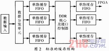
The advantage of this structure is that for each program, there is a separate buffer space for buffering thereof, and each program is relatively independent and does not interfere with each other; in the case where the number of programs is small, the structure is efficient and convenient. Expansion.
However, the problem with the above structure is that if the number of program channels is too large and the input data flow is too large, the number of internal buffers of the FPGA will rise geometrically, the FPGA resources are greatly consumed, the running clock frequency is lowered, and the speed of the system is reduced after the system is integrated.
4.2 Port-fixed MIMO structure buffer Due to the problems of the standard MIMO structure, it is difficult to achieve the application requirements required in this paper, so an improved design proposed here. This design does not cache the DDR logical structure like standard MIMO. Instead, it fixes the DDR high-order address and uses the physical structure cache to store it quickly, as shown in Figure 1.
In this configuration, the external stream processing module first distributes the data stream and the channel number stored in the data stream to the cache RAM and the address translation module, and then the scheduling module dispatches the converted corresponding address pointer and sends it to the DDR correspondingly. The physical storage space and the output port are also only for the physical output port in the same way, which requires a read request queue to send the destination channel to be read in advance. Here, the scheduling module can detect the usage of each channel in real time and distribute the data stream quickly. This kind of structure can reduce the internal RAM consumption of the FPGA by minimizing the internal RAM consumption of the device by inputting hundreds of streams to a physical IP port such as EQAM, and it will not reduce the system performance too much. Moreover, using RAM directly in the front-end data cache without using a FIFO is more advantageous for synchronizing data streams and corresponding addresses.
5 System Test In order to test the accuracy of the design, after embedding the above module into the EQAM system, receiving the IP video data from the network, and detecting the data result by the code stream analyzer, it is found that the data stream packet counter has no error after the DDR buffer. There is no packet loss situation, and the code stream analyzer comes with a player that can play the festival clearly and continuously, as shown in Figure 3. However, during the program conversion process, a PAT error will occur due to different programs, and the error does not affect the normal playback of the program. 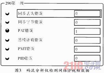
6 Conclusion In this paper, an improved MIMO structure DDR buffer is proposed in this paper, and the implementation functions of the core control module are described. The influence of the improved design on the system is discussed. The final test results also show that the design can be applied to the cache of multi-channel large-capacity video equipment.