How to make PCB imposition? Detailed step decomposition
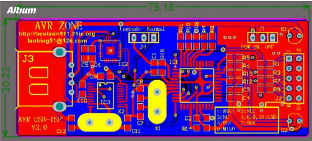
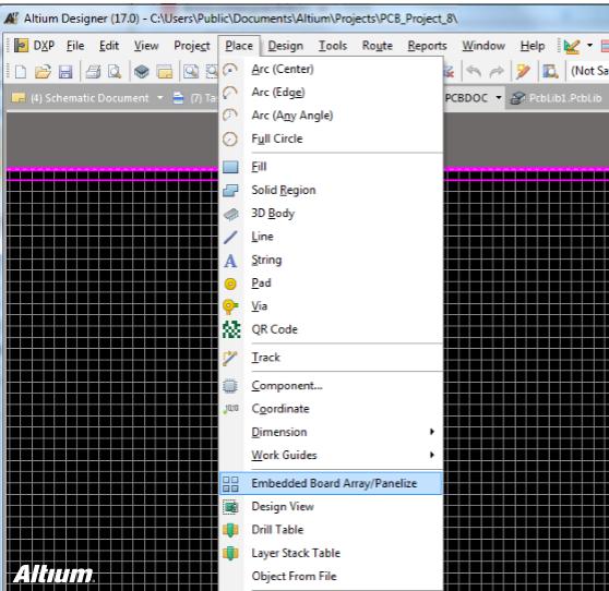
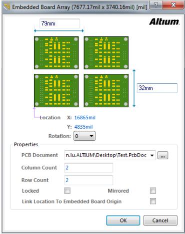
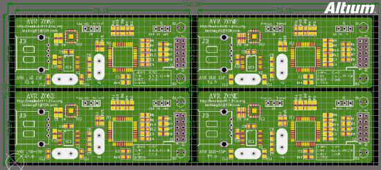
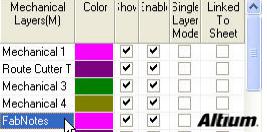
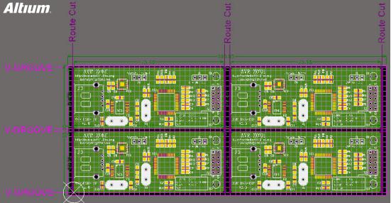
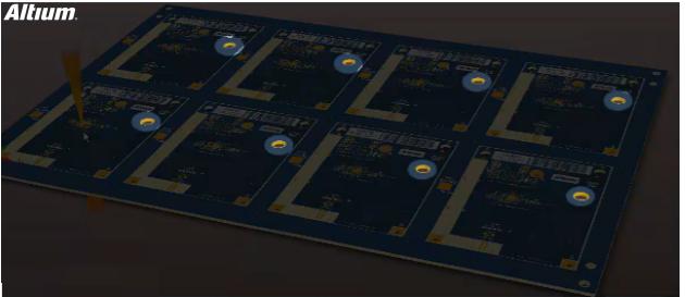
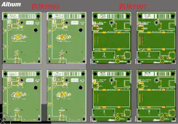
With the continuous development of the entire electronics industry, many products in the electronics industry have established upstream and downstream supporting companies. From a mature product design, design, manufacturing, assembly testing, packaging, wholesaler channels, etc., such an industrial chain is naturally generated in a specific environment. Therefore, the connection between design and manufacturing is extremely close and inseparable. The most important part of electronic products from design to manufacturing is the processing of PCB boards. Most of the bare boards processed by the PCB are to be mounted on the SMT machine. Then the problem has arisen. Nowadays, electronic products are all moving toward small and lightweight. When your design PCB board is particularly small, and some electronic product modules are as small as a few centimeters square, the PCB manufacturing and manufacturing is reversed, but at the PCB assembly stage, the small area is placed on the placement machine for assembly. It brings problems. There is no way to assemble a production line! Here, it is necessary to make a small piece of PCB and make it into a suitable area that meets the requirements of the assembly machine, or to form a yin and yang plate, which is more convenient for patch assembly. In general, the manufacturer of the panel will provide the service of the puzzle, but in the AlTium Designer software design, there are many benefits besides more clearly showing designer's intentions. The benefits are as follows: Can be in the direction you want The puzzle file is associated with the source board, and the source board changes are automatically updated to the puzzle You can put together several different boards You can spell yin and yang (alternating between the front and back) How is AlTIum Designer puzzled?      Here we use an example to introduce the process and operation steps of the puzzle in AlTIum Designer. 1, first determine the size of the board. This can be viewed using Report > Board informaTIon. As shown below, this board is used as an example PCB board with a size of 75.18 x 30.23mm. We want to spell out a 2x2 PCB array in a new PCB diagram. 2. Use File> New> PCB to create a rectangular PCB with a size of 160 x 65mm, two signal layers, no power plane, and through holes. The newly created PCB for the puzzle is as follows and saved. 3, On the newly created PCB, click Place > Embedded Board Array/Panelize. As shown below.       This is our imposition function. Click on it and see the following picture. Output the length and width in the Embedded Board Array window (this parameter is generally slightly larger than the original board. It depends on your needs). In the PCB Document column, select the board PCB file you want to spell. Then enter the number of horizontal and vertical rows of panels to be struck in the Column Count and Row Count row elements. Select 2 here. 4, After setting the above parameters, click OK to place the array board on the PCB diagram. Adjust the position just right. And reposition the PCB origin to the origin of the array board. 5, enter the following layer color manager, rename Mechanical2 to Route Cutter Tool Layer, the line drawn on this layer is defined as the milling cutter through the PCB trace; Rename Mechanical5 to FabNotes, the line defined in this layer is drawn To wash the V-groove (V-GROOVE) traces on the PCB.       The following figure shows the array board with details traced.        Note that we need to draw Route Cutter Tool Layer traces and FabNotes traces on the PCB array board. We need to let the processing plant CAM drawing personnel understand our specific needs and intentions. But specifically, we must take the Cut or V slot, based on our communication and exchange with the board engineer. Here is a schematic diagram. In the end, it is to convert the PCB assembled array board into a processing drawing file such as Gerber. Given to the PCB processing plant, the specific process requirements and details were communicated to the board manufacturer. Patches and source boards are updated synchronously        If you make any changes on the source PCB board, these changes are updated one-click in the PCB board file. For example, as shown below, place a pad in the source PCB.        Then, in the PCB layout file, click Refresh. Each of these boards will have an extra pad. Synchronized with the source board. As shown below. How to put together different PCBs?         To put different PCBs together, you only need to select a certain PCB file and spell out the array. Then select other PCB files and then spell out the array. As shown below.        It should be noted here that for different PCBs to be put together, the number of layers and the thickness of the layers of PCBs that need to be put together must be exactly the same. Can be processed together. If you want to spell a yin and yang board, you can use the panel function to place a panel array first, and then place another mirror array to select the mirror. Also, the yin and yang plates must have the same thickness in each layer. Can be processed together. 76-200Kva Diesel Generator,Volvo Generator,Generator Set,Portable Diesel Generator Shanghai Kosta Electric Co., Ltd. , https://www.generatorksd.com