An embedded network interface design
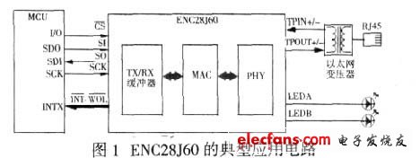
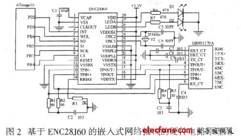
1 Introduction With the advent of the Internet and the rapid development of Ethernet, Ethernet-based device control is increasing. Most of the Ethernet controllers currently on the market use more than 80 pins, such as RTL8019AS, DM9008, and CS8900A. These devices are not only complex in structure, large in size, but also costly in system. Recently, Microchip introduced the world's first 28-pin stand-alone Ethernet controller, the ENC28J60, which provides a low pin count, low cost, and streamlined telematics solution for embedded systems. The Ethernet interface implementation scheme with ENC28J60 as the core is designed, and the design method of the hardware architecture of the system is described. Based on a brief introduction to the structure, function and peripheral circuits of the Ethernet controller ENC28J60, the SPI communication between ENC28J60 and Atmega16 is described. This solution not only has low cost, but also achieves a transmission rate of more than 500Kbps, which satisfies the Internet control requirements of embedded systems. 2 ENC28J60 network interface architecture The ENC28J60 is a standalone Ethernet controller with an industry standard Serial Peripheral Interface (SPI). It complies with all IEEE 802.3 specifications and employs a series of packet filtering mechanisms to limit incoming packets. It also provides an internal DMA module for fast data throughput and hardware-supported IP checksum calculations. Communication with the host controller is accomplished via two interrupt pins (INT and WOL) and SPI pins (SO, SI, SCK, CS) with data transfer rates up to 10 Mb/s. Two dedicated pins (LEDA, LEDB) Used to connect LEDs for network activity status indication. Figure 1 shows a typical application circuit for the ENC28J60. The ENC28J60 consists of seven main functional blocks: the SPI interface, which acts as the communication channel between the host controller and the ENC28J60; the control registers for controlling and monitoring the ENC28J60; the dual-port RAM buffer for receiving and transmitting data packets; Access to the RAM buffer when the DMA, transmit and receive modules make a request; bus interface, parsing data and commands received via SPI; MAC module: implementing IEEE 802.3 compliant MAC logic; PHY module, pair The analog data on the twisted pair is encoded and decoded. The ENC28J60 also includes other support modules such as an oscillator, an on-chip voltage regulator, a level shifter (providing I/O pins that accept 5V), and system control logic. According to the above description, ENC28J60 is very suitable for embedded network interface, and has broad application prospects. 3 ENC28J60 application in embedded network interface 3.1 hardware circuit design The ENC28J60 can be used to form network terminal nodes with different functions, such as network servers, Internet-enabled devices, and remote monitoring (data acquisition, diagnostic) devices. Figure 2 shows the hardware circuit schematic of the embedded network interface based on ENC28J60. The circuit has: 2 LED status indicators are mainly used to display the network connection status, including whether the PHY conflicts, whether the connection is established, whether to receive data, connection speed, duplex mode, etc.; Required bias resistor R3 (2kΩ, accuracy is 1%); high-speed LAN electromagnetic isolation module (ie RJ45 Ethernet interface), in application, the physical port of ENC28J60 must be in accordance with IEEE802.3 physical layer specification when connecting with isolation transformer HR901170A, such as RJ45 jack and isolation transformer The spacing should be as small as possible, and the output and input differential signal pairs should be well isolated. The main controller in the circuit uses Atmel's ATmega16 microcontroller with advanced RISC (Reduced Instruction Set Computer) architecture, 16 kB programmable Flash memory, 512 B EEPROM and 1 kB of on-chip SRAM with rich peripheral interfaces. Its SPI interface allows ATmega16 to communicate with peripherals at high speeds. In this design, the ATmega16 SPI is configured in master mode and the ENC28J60 is slave. The SPI operating mode of ATmega16 is set by CPOL and CPHA. According to the SPI read/write timing of ENC28J60, the SPI working mode of ATmega16 should be set to mode 0. ATmega16 synchronizes with the CS pin of ENC28J60. The SPI clock is initiated by the data written to the SPI Transmit Buffer register. The data transmission order on the SPI MOSI (PB5) pin is controlled by the DORD bit of the SPCR register. When set, the LSB (lowest bit) of the data is transmitted first, otherwise the data is The MSB (most significant bit) is sent first. We choose to send the MSB first, and the received data is transferred to the receive buffer register, and the CPU performs right alignment to read the received data from the receive buffer. It should be noted that when multiple data needs to be read from the ENC28J60, even if the ENC28J60 does not require the data of the ATmega16 serial output, write a data to the SPI Transmit buffer to start the SPI interface clock before each data is read. Since the SPI system has only one buffer in the transmit direction and two buffers in the receive direction, it must wait until the shift process is completed before writing to the SPI data register. When receiving data, , the current received data needs to be read by accessing the SPI data register before the end of the next byte shift process, otherwise the first data is lost. 3.2 ENC28J60 Software Initialization The device must be initialized before sending and receiving packets using the ENC28J60. Depending on the application, some configuration options may need to be changed. Initial setup tasks include receive and transmit buffers, receive filters, crystal start times, MAC registers, and PHY registers. Before initializing the chip, turn off the interrupt input of the microcontroller, give a continuous low-level reset signal to the RESET pin, and then set the corresponding register. After setting all the required registers, judge whether the clock start flag in the Ethernet status is set, and then open the interrupt. After the system is initialized, it enters the main program loop, including the control function of the microcontroller and network data transmission. For the Ethernet transmission part. There are two main functions: one is to encapsulate and send the data to be sent according to the Ethernet data frame format; the other is to unpack the received Ethernet data frame and use it for the application.
Float Charge
Nickel Cadmium Battery – 1.30V per cell
This will enable the battery to recover its capacity quickly and reduce the water consumption. In this aspect, it will reduce the topping up frequency and storage of water.
Boost Charge
Nickel Cadmium Battery – 1.60 V per cell
Equal Charge
Nickel Cadmium Battery– 1.65 V per cell
Nickel Cadmium Battery Charger Nickel Cadmium Battery Charger,Smart Battery Charger,Electric Stacker Battery Charger,Rechargeable C Batteries Xinxiang Taihang Jiaxin Electric Tech Co., Ltd , https://www.chargers.be