Reasons for PCB board clamping
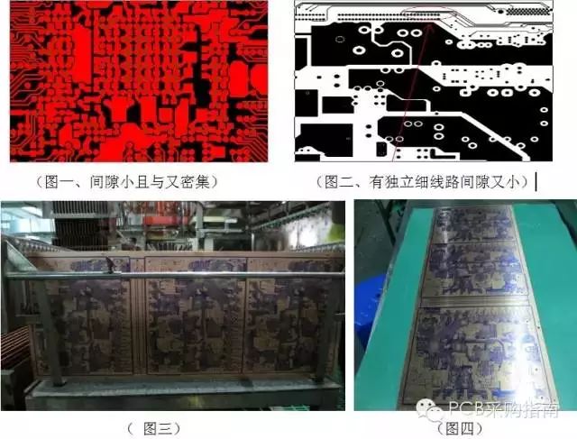
I. Introduction: With the rapid development of the PCB industry, PCBs are gradually moving towards the development of high-precision fine lines, small apertures, and high aspect ratios (6:1-10:1). Hole copper requires 20-25 Um, and DF line spacing is less than or equal to 4 mil. General production PCB companies have electroplating film problems. The film will cause a direct short circuit, affecting the yield of the PCB board once the AOI is inspected, and the serious film or the number of points that cannot be repaired will directly lead to scrapping. Second, graphic plating film problem illustrated: PCB plate clamping principle analysis 1 The plating thickness of the pattern plating is larger than the dry film thickness, which will cause the film to be trapped. (General dry film thickness of PCB factory 1.4mil) 2 Pattern plating copper thickness plus tin thicker than the dry film thickness may cause clip film. Third, the PCB board clamping film analysis 1. Easily clips pictures and photos Figure 3 and Figure 4, from the physical board photos can be seen that the line is more dense, engineering design layout length and width ratio difference larger adverse current distribution, D / F minimum line gap is 2.8mil (0.070mm), the minimum hole is 0.25mm, Board thickness: 2.0mm, aspect ratio 8:1, hole copper requirements> 20Um or more. It belongs to the process difficulty board. 2. Analysis of the cause of the film 1 graphics plating current density, thick copper plating. 2 There are no clip strips at both ends of the fly bar, and a thick film is coated in the high current area. 3 The firebrake fault has a larger current than the actual production board. 4C/S surface hangs against S/S surface. 5 spacing is too small 2.5-3.5 mil spacing plate clamp. 6 The current distribution is not uniform, and the copper plating cylinder has not cleaned the anode for a long time. 7 wrong current (input wrong type or wrong board area) 8 Equipment failure Bad PCB protection time is too long in the copper cylinder. 9 The layout design of the project is irrational, and there are errors in the effective plating area provided by the project. 10 PCB board line gap is too small, difficult board circuit graphics special easy film. Fourth, the film to improve the program 1. Decrease the current density of the graph and properly extend the copper plating time. 2, the thickness of the plate plating copper appropriate thickening, appropriate to reduce the copper density of the figure plating, the relative reduction in the thickness of the plating copper. 3. The copper thickness at the bottom of the pressure plate is changed from 0.5OZ to 1/3OZ copper pressure plate at the end. The copper plating thickness of the plate is about 10 Um thick, reducing the current density of the picture and reducing the thickness of the plated copper. 4, for the spacing of <4mil board procurement 1.8-2.0mil dry film trial production. 5, other programs such as changing the layout design, modify the compensation, shift wire gap, hole ring and PAD can also reduce the relative generation of the film. Fifth, the line gap small easy to clip plate plating production control method 1. FA: First try a clip on the ends of a flying plate and fly bar. After the copper thickness, line width/line spacing, and impedance are qualified, the AOI is etched through a flying plate, and if the phenomenon of film clamping is found, adjust it immediately. Current retry FA. 2. Prohibited film: For the board with D/F line gap <4mil, the filming speed of etching is appropriately slowed down. 3, FA personnel skills: easy to note the current density of the board to pay attention to the current density assessment, the general board minimum line gap <3.5mil (0.088mm) of the board, figure electroplating copper current density control at 12ASF is not easy to produce clip film. In addition to the line graph, a particularly difficult board is as follows: The minimum line gap of the graphics board D/F is 2.5 mil (0.063mm). Generally, the uniformity of the manufacturer's electroplating line is good and it is difficult to escape the fate of the film. It is recommended to use the 10ASF current density test FA. The minimum line gap of the graphics board D/F is 2.5 mil (0.063mm). There are many independent lines and uneven distribution. In general, the plating line uniformity of the general manufacturer is better, and it is difficult to escape the fate of the film. The current density is 14.5 ASF*65 minutes to produce a clip film. It is recommended to use a ≦11 ASF current density test FA. Sixth, the main reason I am engaged in PCB years of experience in the process of summing up, basically every PCB factory to do the line width of the small gap of the board will have more or less clamping problems, the difference is that each company's poor proportion of clips, some companies folder There are few membrane problems, and some companies have many membrane problems. Analyze the following factors: 1, each company's PCB board structure type is not the same, PCB manufacturing process is not the same difficulty. 2. Each company's management model and practices are different. 3. Based on my many years of accumulated experience, the first thing to note is that for a small board with a small wire gap, only a small current density and an appropriate length of copper plating time should be taken into consideration. The current indication is based on experience to evaluate the use of current density and copper plating time. Pay attention to the method and operation method of the splint. For the board with the minimum line spacing ≤ 4mil, the FA-fly plate must pass the AOI to check whether there is a film clamping problem, and at the same time, it plays a role of quality control and prevention, so that the clamps are produced in mass production. The chance of the film will be very small. Personally think that good PCB quality not only has experience and skills, but also a good way. Another point depends on the implementation of the personnel in the production department. The electroplating is different from the electroplate plating. The main difference lies in electroplating the circuit patterns of various types of boards. Some circuit board patterns are not evenly distributed. In addition to the fine line width, there are sparse and isolated wires. Separate holes for various special circuit patterns. Therefore, the author prefers to use FA (current indication) skills to solve or prevent the problem of thick film coating. Improve the speed of action is small and effective, prevention effect is obvious. Small computer system interface (SCSI) is an independent processor standard for system level interfaces between computers and intelligent devices (hard disks, floppy drives, optical drives, printers, scanners, etc.). SCSI is an intelligent universal interface standard. HPCNS SCSI Section ShenZhen Antenk Electronics Co,Ltd , https://www.antenk.com


