Silicon substrate PK sapphire substrate, winning and losing geometry?
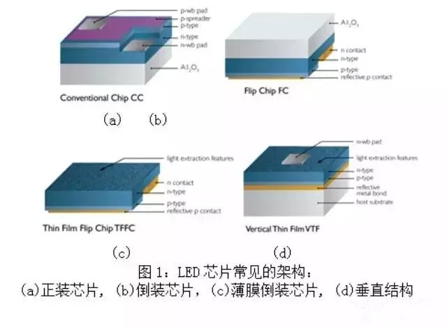
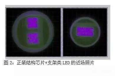
The chip structure of gallium nitride-based blue/white LEDs is strongly dependent on the substrate material used. At present, most manufacturers use sapphire as the substrate material, and the chip structure is mainly divided into four categories, as shown in Figure 1: (Click to enlarge) Positive chip structure Such chips are widely used in low- and medium-power package products, and the advantages are low price; the disadvantage is that the sapphire has poor thermal conductivity, so the heat dissipation of the chip is poor, and the conductivity of the P-type material is also poor, so the injection current is limited. In addition, the chip is illuminated on five sides, and it is usually required to place the chip in the holder. As shown in FIG. 2, the opening area of ​​the reflector is much larger than the area of ​​the chip, resulting in low luminous flux per unit area, and the color uniformity of the chip surface is very poor. The chip is blue above the front and yellow on the outer ring. This is the reason why yellow circles appear in use, such as spotlights, flat lights, etc. Flip-flop structure In order to overcome the shortcomings of poor heat dissipation and limited injection current of traditional dressing structures, some researchers have proposed a flip-chip structure. Heat can be transferred directly from the chip to a substrate such as ceramic without passing through a sapphire substrate with poor thermal conductivity, so the injection current can be significantly increased; the luminous flux per unit area can also be significantly improved. The disadvantage is that the chip is illuminated on five sides, which brings a lot of inconvenience to the occasions that require precise secondary optical design, such as small-angle spotlights, mobile phone flash, car lights, ultra-thin backlights and flat lights. In addition, there are also formal dresses. The problem of uneven color color faced by the five-sided light-emitting chip. Film flip structure In order to solve the problem of the flip-chip structure, a film flip-chip structure has been proposed. On the basis of flip chip, the sapphire substrate is removed by laser stripping technology to obtain a single-sided light-emitting film chip. The thin film chip has high light extraction efficiency and concentrated light directly on the chip, which is advantageous for secondary optical design, and also has very good surface color uniformity. However, the complicated laser stripping technology is used, the cost is high, the yield is low, and the chip itself is prone to defects. In addition, due to the flip-chip structure, there is a gap between the chip and the (ceramic) substrate, which is somewhat reduced. The thermal conductivity of the chip; at the same time, due to the very thin chip, it is prone to chip cracks, leakage and other problems in use. Vertical structure Corresponding to the film flip-chip structure, there is also a vertical structure chip, similar to the flip chip, the sapphire substrate is stripped, and the high-reverse material is plated on the bottom of the chip, and then the conductive and thermally conductive substrate material is added, so that the chip In addition to the advantages of the single-sided light-emitting chip, it also has good thermal conductivity and electrical conductivity, and the reliability is also very high. The vertical structure is currently the most widely used thin film chip structure, but since the sapphire substrate needs laser stripping, the yield is low and the cost is high, which limits the wider application of the vertical structure chip. Transformer insulated Laminated Wood Round Bar is made of laminated wood, with light and lightweight texture, which is not easy to twist and crack. Laminated Round Bar,Transformers Wood Bar,Laminated Wood Round Bar,Transformers Insulation Laminated Wood Bar Yingkou Dongyuan Electrical Insulation Board Co.,Ltd , https://www.dy-insulation.com