Mobile processors move toward higher integration
As a mobile advertising display, Vehicle LED Display has precise advertising positioning and is widely used in public transport, taxis, case trains and family cars. It is widely used in outdoor image advertisement, information publication, activity advertisement, mobile background stage, information media and live broadcast of events, etc. its products are effective and flexible and widely used.
Features of Vehicle Led Display:
1. There is a unified operation background. Through GPS, you can know the specific location of each on-board screen. GPRS wireless replacement product content can play all the specified content partially. The above operations can be realized by computer and mobile phone
2. Mobile advertising has stronger communication and better effect. For vehicle mounted display screen, it has been in a state of motion, and advertising information has been more widely spread, with stronger communication ability and larger coverage area than fixed platform.
3. Vehicle Led Display adopts high brightness LED lamp beads, which can be seen clearly in the sun. The product has UV resistance in the sun, and the protection level reaches IP65, which is suitable for all-weather playback.
4. Ultra thin design of the product, allowing disassembly and assembly, reducing the space occupied in the car
5. Product module design, reliable and stable performance, power supply, system card, separate device, more stable product, more convenient maintenance
6. Led vehicle screen with GPS function can accurately know the screen position and operation status, including vehicle speed, driving direction, alarm status, etc.
7. Vehicle LED Display add brick and tile to the bright urban environment and become a beautiful scenic spot.
Original title of structure:
1. The screen adopts wide voltage, which can be applied to any vehicle in any occasion.
2. Single box design, according to customer requirements, can be iron box, can be aluminum box.
3. The system adopts group network function, which can control all vehicle screens individually. Even if the screen body is not in the same city, it can send specified and information through GPRS.
4. The screen body has an understanding of the lifting device, and the height can be adjusted according to the customer's requirements.
Vehicle LED Display Led Display Panel,Vehicle Led Display,Led Screen Truck,Car Led Display Shenzhen Vision Display Technology Co,.LTD , https://www.ledvdi.com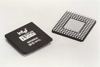 Mobile device specification upgrades drive processor design architecture changes. Mobile devices are increasingly demanding for lightness, thinness, power consumption, and cost. In addition to stimulating large manufacturers such as MediaTek and Samsung to rush to use the big.LITTLE size core architecture to design next-generation processors, they also drive semiconductor manufacturers to step up research and development of 3D ICs to meet Market demand for higher integration processors.
Mobile processor system single chip (SoC) with big.LITTLE architecture will be fully released. With mobile devices increasingly demanding performance and power consumption performance, processor companies including MediaTek, Samsung, and Renesas Mobile have successively used ARM's big names. .LITTLE size core and mix architecture, the development of a new generation of multi-core processors, and will launch large-scale products this year, to seize the high-end smart phone market.
In addition, mobile phone internal processors, power management chips (PMICs) and touch ICs are accelerating their integration. The evolution of semiconductor processing alone has gradually fallen short of IC designers' substantial reductions in chip size and savage demand for lower costs, making semiconductor supply chain suppliers more attractive. Increasing competition for 3D IC (3D IC) R&D investment to match the introduction of advanced processes and achieve higher integration of wafer solutions.
Grab high-end smartphone big.LITTLE processor
Lin Xiuping, ARM mobile communication and digital home marketing manager, believes that heterogeneous system architecture will also be the focus of future SoC development. ARM has joined relevant standards organizations to develop specifications. He also said that due to the continuous upgrading of the functional specifications of smart phones, and at the same time, it is necessary to take into account the endurance. Therefore, ARM has not only departed from the old multi-core processor design method, but also introduced a big.LITTLE size core architecture to work on mobile phones with different performance requirements. Tasks are dealt with with the best core, thereby reducing the system burden.
The concept of big.LITTLE is exactly the same as that of a Hybrid Electric Vehicle (HEV). It can switch operating modes at any time to achieve better mobile phone performance and power consumption specifications. If the mobile phone is in the standby or light load state for more than 70% of the time, it will be more than sufficient to deal with the low-power core. As for the few situations where high computation is required, the high-efficiency core will increase the clock speed. At this stage, big.LITTLE not only has licensed nearly 10 processor manufacturers, including mobile phone brands such as Samsung, Nokia and Huawei have also planned to introduce new products, indicating that this innovative SoC architecture has become a mobile device. Supply chain operators lay emphasis on the layout.
In addition to mobile phone and tablet chip manufacturers gradually moving closer to the big.LITTLE architecture, Japan's TV SoC developers and ARM architecture server chip suppliers have already planned to import big.LITTLE solutions to reduce power consumption under low loads. the amount.
Lin Xiuping pointed out that this year will be the first year of the big.LITTLE multi-core processor. It will initially lock high-end mobile phones. After wafer prices decline next year, it can be expected to penetrate into the mid- to high-priced mobile phone market. The next 1-2 year big.LITTLE program will also be favored by more application processor developers, and further expand its influence in tablet devices.
In fact, MediaTek has plans to rely on the big.LITTLE technology to fully develop its presence in the tablet market. Optimistic about flat-panel market growth potential, MediaTek began to expand investment in the development of flat-panel wafers in the second half of last year, and at the beginning of this year, Acer and other brand factory orders have been gradually performed, the performance is dazzling; in the third quarter of this year will re-offer two 28 nm (nm ) Quad-core processors - MT6582 and MT8135, one of which uses the big.LITTLE architecture.
Expansion of flat-panel market accounts for MediaTek's push to size nuclear APs
Xie Qingjiang, general manager of MediaTek, stated that MediaTek’s current performance in the flat-panel chip market is much better than expected at the end of last year, and two new products will be available in the second half of this year, which will help to continuously expand the penetration rate. Therefore, the company has recently taken 2013. The annual flat plate wafer shipment target has been substantially raised from 10 million to 10 million wafers to 10 to 15 million; and the market development strategy of diversified customers has been positively involved in mobile devices and individuals. Computer (PC) brand manufacturers and information service providers (such as e-book readers).
Xie Qingjiang emphasized that the MT6582, a new-generation quad-core ARM Cortex-A7, will be mass-produced at the end of the third quarter of this year, and will introduce 28nm process technology. At the same time, MediaTek is also developing the big.LITTLE SoC--MT8135, which will integrate two high-efficiency Cortex-A15 and two low-power Cortex-A7 cores in a hybrid design to meet the needs of high-end flat-panel applications. Performance, size and power requirements. At present, the program has begun to provide samples of brand customers, and it is expected to produce a small quantity in the third quarter.
Obviously, MediaTek entered the flat-panel market with a four-core mobile phone processor platform at the end of last year, and even overclocking the quad-core application processor for tablets was only a small test. Two more advanced flat-panel chips will be fully launched in the second half of this year. . At present, the proportion of the company’s flat-panel wafers has been more than 50% of the shipment to brand manufacturers, and the market share is continuing to rise; in the second half of the two new products with better price/performance ratio, it is expected to attract more brands, information Services are even favored by white-label companies.
Xie Qingjiang pointed out that at the end of the year, its first LTE multi-band multi-mode chip will also be available, and will use a quad-core application processor to assist customers in upgrading their 4G specifications for new products. In 2014, it will release a quad-core SoC that integrates an application processor with an LTE baseband processor.
Responding to the needs of the IC design industry for the big.LITTLE architecture, Lin Xiping stressed that from the Cortex-A7/A15 onwards, ARM's future processor cores will be based on the support of big.LITTLE. At the same time, more hardware and software development resources will be invested. Accelerated the next generation of big.LITTLE program. Among them, three-dimensional (3D) transistor or 3D IC design will be an important future direction for development. At present, ARM has jointly developed 16-nanometer fin-type transistor (FinFET) and a three-dimensional wafer stacking process with TSMC and a number of wafer manufacturers.
Mobile phone chip crazy integration 3D IC non-playable
The rise of affordable high-profile smart phones accelerates internal chip integration and process evolution; however, the cost of R&D for processes below 20nm is extremely high, but the resulting size and power reduction benefits are relatively limited, so semiconductor manufacturers have launched 3D simultaneously. IC development to achieve a higher level of wafer integration, of which Samsung has been the first to announce mass production next year.
According to Cai Zongting, a researcher at the Semiconductor Research Center of TPI, the 2013-2015 mobile phone internal chips will continue to be integrated with the application processor as the core, and will introduce advanced processes below 20nm, including baseband processors, networking modules, and Radio frequency (RF) transceivers will all be combined into one. In addition, power supplies, audio and video, and touch ICs will also be gradually integrated into SoCs; and various MEMS sensors will be packaged to form sensor hubs. From the twelve in 2012, it quickly reduced to about six (Table 1).
As everyone knows, the key to improving the degree of wafer integration is process miniaturization. However, after fabs jumped from 28 nm to 20 nm, they face the limits of the physical properties of semiconductor materials and the huge investment in equipment costs. However, it was only able to fall by 3.34%, far behind the level of 10?33% of the previous generations; and the area was only reduced by 28%, which is not as good as the 40% improvement of each previous generation evolution; various factors will lead to 20nm approximately. Eight-inch wafer prices soared 35.42%.
As the ROI on process miniaturization gradually becomes unbalanced, the semiconductor company is switching to 3D ICs. At SEMICON Singapore 2013, Samsung and Qualcomm all unveiled a new generation of three-dimensional stacked design of Wide I/O memory plus logic chips. The former is also equipped with memory and application processor technology. The company announced that it will start production in 2014.
For the packaging and testing industry, 3D ICs will be an important weapon for consolidating future revenues. Cai Zongting analyzes that once the packaging requirements for standard mobile phone chips are halved, it will greatly affect the sources of the packaging and testing plant's revenue, thus stimulating counterfeit goods and STATS ChipPAC, and actively deploying 3D IC packages with high technical content and high gross margin. Technology, including wafer-to-surface stacking (F2F Stacking), 2.5D Interposer, etc.
In addition to the packaging and testing plant, TSMC has also spurred CoWoS (Chip on Wafer on Substrate) process business to attract equipment manufacturers to step up deployment of new programs. Cai Zongting revealed that 3D ICs have to be perforated (TSV) and the process is very time-consuming and costly; for this reason, Tokyo Electron has recently released a new process and improved Etching, Cleaning and Liner equipment, saving wafer barriers, chemical mechanical polishing (CMP) production schedule, so that 3D IC wafer production doubled. At the same time, as Taiwan Semiconductor Manufacturing Co., Ltd. is gradually increasing the proportion of its purchases in the field, Taiwan-based Shangsu has also invested in research and development of 3D IC etching equipment and actively seeks orders.
Cai Zongting emphasized that the development of mobile device parity is highly improbable. Taking Apple as an example, since the launch of the iPhone 4 with a price of 650 US dollars in 2010, the prices of the next two generations of products have maintained the same level, but the display panel and processing Hardware specifications such as devices and memory have leapfrogged; the same situation has also occurred in other Android mobile phone brands, thus aggravating wafer maker product integration and production cost pressures. 

