Fuwei Group launches Invensense, Leadcore, Qualcomm (Summit), RFMD smart phone solutions
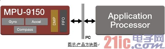
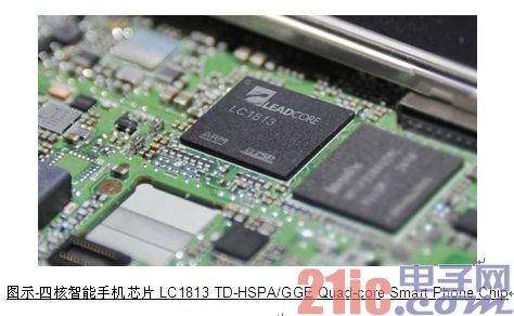
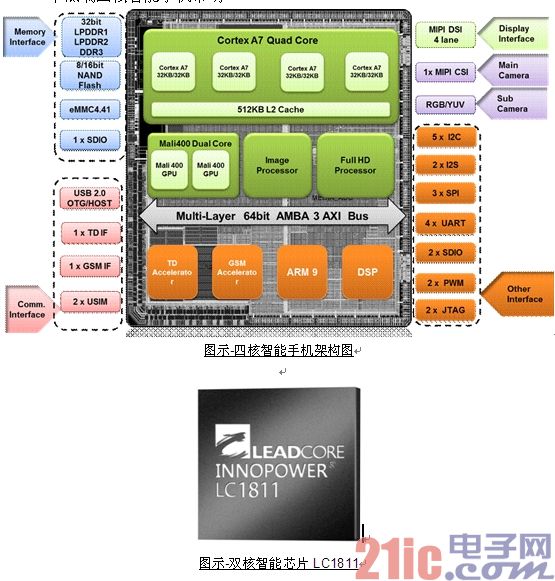
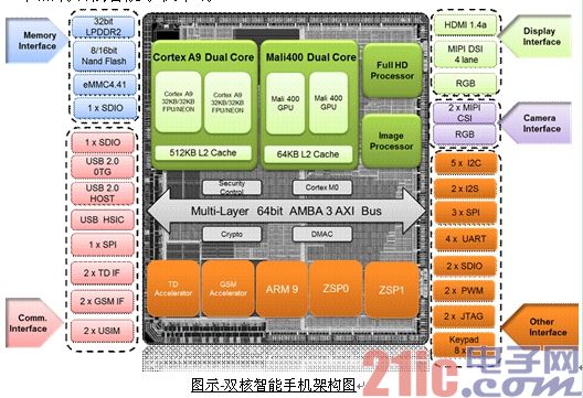
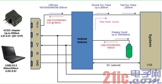
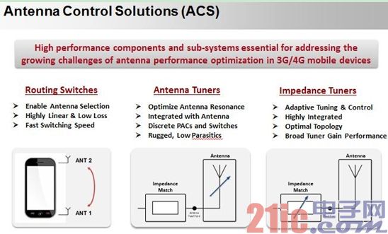
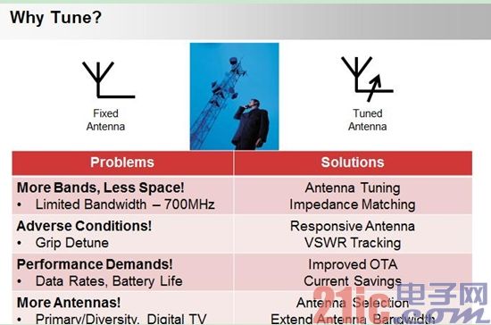
21ic News Great Alliance Holdings announced that its Fuwei Group has launched smartphone solutions from InvenSense, Leadcore, Qualcomm (Summit), RFMD and other vendors. This article refers to the address: http:// InvenSense MPU-9150 nine-axis (gyro + accelerator + electronic compass) MEMS motion sensing tracking (Motion Tracking) device InvenSense, represented by Fuwei Group of the United Nations General Assembly, launched the world's first nine-axis motion tracking tracking device (MPU-9150), which is designed for low-power applications such as smart phones, tablet computers, and wearable sensors. Cost, low cost, high performance consumer electronics device design. The device is a system-in-package (SiP: System in Package) product that integrates two chips: an MPU-6050 with a three-axis gyroscope, a three-axis accelerator, and a built-in high-performance digital motion sensing processor (DMP: Digital Motion Processor); the other is the AK8975---three-axis digital electronic compass. The Motion Apps platform with the MPU-9150 includes Motion Fusion and run-time calibration firmware, allowing manufacturers of motion sensing products to save time. The cost and hassle of selecting, testing, and integrating individual devices in the system phase, and ensuring sensor fusion algorithms and calibration procedures to provide optimal performance for the consumer (optimal performance) ). Leadcore quad-core smartphone chip LC1813 with dual-core smartphone chip LC1811 Leadcore (Lianxin), represented by Fuwei Group of the United Nations General Assembly, launched its quad-core smart chip LC1813 and dual-core smart chip LC1811. Based on a 40nm process, the LC1813 features a quad-core ARM Cortex A7 and dual-core GPUs with powerful CPU and GPU capabilities, a highly integrated PMU, Codec chip, and a high-performance RF chip to improve product launch efficiency. In addition to the huge improvement of the chip hardware architecture, it is excellent in multi-tasking and application performance. It adopts Android's latest 4.2 version of the operating system. The smart terminal LCD presents the highest resolution for WXGA's high-definition visual experience. The 13-megapixel ISP camera capability is superficial. Features such as smile recognition, digital zoom, auto focus, and macro mode are comparable to digital cameras. At the same time, it supports “Wi-Fi Displayâ€, which can simultaneously output wireless HD video to meet the family audio and video entertainment experience; Waiting for features makes it easier to balance business and life needs. LC1811 is an upgraded version of Lianxin Technology's first dual-core chip LC1810. It uses ARM dual-core Cortex A9 and dual-core GPU, 1.2GHz frequency, with downlink 4.2Mbps/upstream 2.2Mbps TD-HSPA+ carrying capacity, and supports 1080P video codec. Focusing on providing powerful performance, LC1811 focuses on cost management and targets the low-end and mid-end smart terminal market. It shows that terminal manufacturers quickly introduce cost-effective smart products to help popularize TD smart terminals. Technical indicators: • Quad-core Cortex A7 1.2GHz • Dual-core GPU Mali400, 832M Pix/s, 45M Tri/s • Support for LPDDR/LPDDR2/DDR3 • 1280x800 WXGA resolution • 1080P multimedia playback and camera capabilities • 13 megapixel camera processing capability • Wi-Fi Display Wireless Full HD Video Output • TD-HSPA/GSM+GSM dual card dual standby • 40nm LP CMOS process • 12mm x 12mm BGA package • Support Android 4.2 Targeted market: • Low-end quad-core smartphone market Technical indicators: • Dual core Cortex A9 1.0/1.2GHz • Dual-core GPU Mali 400 832M Pix/s, 45M Tri/s • Support for LPDDR/LPDDR2/DDR3 • 1280x800 WXGA resolution • 1080P multimedia playback and camera capabilities • 8 megapixel camera processing capability • HDMI 1.4a 3D Full HD Video Output • TD-HSPA/GSM+GSM dual card dual standby dual pass • 40nm LP CMOS process • 12mm x 12mm BGA package • Support for Android 4.0 Targeted market: • Low-end dual-core smartphone market Qualcomm (Summit) Battery Charging IC Solution SMB348 (1.5A) / 358 (2A) Like all Qualcomm (Summit) battery charging IC solutions, the SMB348/358 chip has the same high integration and high flexibility design capabilities. Digital I2C control and non-volatile configuration while maintaining the simplicity of independent operation or the flexibility of host control. Parameters and functions can be easily reconfigured to suit a variety of applications or system operating modes. High integration and high frequency operation reduce external use parts, and the CSP package also helps with smaller solution sizes. The SMB348/358 is the ideal charging and system power solution for virtually any portable product that uses high-capacity batteries and requires reliable fast charging. Introduction: The SMB348 and SMB358 are programmable charging ICs that can be used in single Lithium-ion/Lithium-polymer battery charging designs, making them ideal for a wide range of portable applications. This IC provides a simple and efficient way to charge high-capacity Li-Ion batteries and provide system power through the input power of a USB or AC transformer. The SMB348 and SMB358's high-efficiency switching modes operate differently than traditional linear charging ICs, solving the problem of low charging current and heat. In addition, its programmable switching architecture avoids USB input current limitations and provides faster charging. USB and AC input current limits up to 2.0A and charge currents up to 2.0A (SMB358) and 1.5A (SMB348). These products can manage two independent outputs: battery charging and system power. This allows the system to start up immediately even when there is no battery or the battery is over-discharged. The internal hardware design of the SMB348 and SMB358 is also available with a +5.0 V/900mA power supply for external USB OTG devices via the battery, as well as USB-ACA standards. Charging control includes input current limit (supports USB2.0 and USB3.0), slow charging, pre-charging, constant current/constant voltage charging, floating charging and termination/safety settings all pass through I2C/SMBus It is set up and stored in the non-volatile memory in the IC, which truly realizes a flexible and flexible solution. The size of the fast charge current can be set via I2C. An external enable pin is also provided to set the charge to suspend or put it into sleep mode and built-in reverse current blocking to prevent accidental battery discharge. These two products offer a variety of protection features such as battery, charger, input circuit (overcurrent, low voltage / over voltage, safety timer, floating charging voltage and charging current, floating charging voltage compensation and thermal protection) . The “STAT†pin can also be used to monitor the state of charge. The operating voltage is +3.6V to +6.2 V and provides overvoltage protection of +20 V. Features: • Provide efficient battery charging and solve hot problems • Maximum charging current • SMB348: 1.5A (max) • SMB358: 2.0A (max) • Automatically detects USB/AC/DC transformer input current and limits its maximum safe chargeable current • Automatic power source detection (in accordance with USB charging specification BC1.2) • USB and AC input input current is programmable (in accordance with USB2.0/3.0) • Through the "Turbo Charge" technology, the maximum 700mA charging current is from 500mA USB port or 2000mA from AC transformer Control via the input and output current paths "Current Path" allows the system to be powered up immediately without a battery or if the battery is already over-discharged. • USB-OTG +5.0V/900mA power supply available for external OTG devices or for HDMI/MHL power supplies • Floating voltage and charge current compensation to support JEITA and JISC 8714 • 1.5MHz or 3MHz switching operating frequency reduces external part volume • Input operating voltage range: +3.6 to +6.2V • +20V input voltage (non-operating mode) provides overvoltage protection • Almost all required parameter settings can be digitally controlled via the I2C interface Main application market: Smartphone, Wireless Router, Tablet PC, DV, DSC, Handheld GPS, MID, Portable Media Player, Portable Game Console, etc. Development environment and software programming: In order to accelerate the development of customer products, Qualcomm provides customers with SMB348/358 evaluation board and software with graphical user interface (GUI). Designers can use its rapid development features and advantages to design a prototype battery in a short time. A charging solution, a complete development tool that allows designers to easily design the charging functions and behaviors they need for their systems. The SMB348/358 design kit includes menu-driven Microsoft Windows graphical user interface software auto-programming tasks, including USB to I2C's Dongle and computer links. Once the customer completes the design, the SMB348/358 automatically generates the HEX file and is used for pre-shipment burning. Qualcomm also assigns a unique item number to this HEX file to avoid mixing. package: The SMB348 and SMB358 are available in two packages with operating temperatures from -30°C to +85°C. • CSP: 2.5mm x 2.4mm, 30-Ball. • QFN: 4mm x 4mm, 24-Lead. Note: Summit Microelectronics was acquired by Qualcomm Incorporated on 2012-Jun-18th. RFMD launches revolutionary product Antenna Control Solutions RFMD's latest antenna control solution (Antenna Control Solutions), which is represented by Fuwei Group, is able to reduce the overall power consumption and volume of the antenna. In addition, the SW compilation function can be used to simplify the RF front-end module. (FEM) design, and achieve antenna frequency adjustment, adjustable impedance matching. The solution was launched to meet the needs of greater space and bandwidth. RFMD has another FDD, TDD-LTE & TD-SCDMA PA with dual RF input & dual RF output for 4G. In addition to supporting multi-mode multi-band, it also has power-saving miniaturization features, providing customers with a variety of specifications.
About PEW Enameled Copper
Wire.
According to design of motor, transformer and
high-speed winding machine, PEW product has the advantages of good paint film
continuity, good flexibility and adhesion. high surface strength. breakdown
voltage is increased by 60% compared with national standard. Suitable for
manual and automatic winding machine .
Oxygen free copper covered polyester painting, Inner packing PT25/60/90/200 Plastic Spool.Outer packing: Carton box + Mooden box.
Insulated Copper Wire,Pew Enameled Copper Wire,Polyester Enameled Copper Wires,Enameled Copper Magnetic Wire HENAN HUAYANG ELECTRICAL TECHNOLOGY GROUP CO.,LTD , https://www.huaonwire.com